
When people talk about multi-chiplet AI accelerators, the conversation almost always centers on the die-to-die interconnect: UCIe bandwidth, HBM stacking, package substrate routing, and silicon interposer performance. The assumption is that chiplets communicate through physical conductors — traces on a substrate, through-silicon vias, or micro-bumps.
A paper from January 2025 (arXiv:2501.17567) asks a different question: what if some of those chiplet-to-chiplet communications went through the air?
This is the kind of idea that sounds absurd until you look at the engineering constraints carefully. The paper, "Exploring the Potential of Wireless-enabled Multi-Chip AI Accelerators," examines wireless technology as a complement to wired interconnects in multi-chiplet packages — not as a replacement, but as an additional communication channel for specific traffic patterns. The results are more compelling than the premise might suggest: 10% average speedup across AI workloads, up to 20% maximum speedup on communication-heavy workloads.
The Wired Interconnect Bottleneck
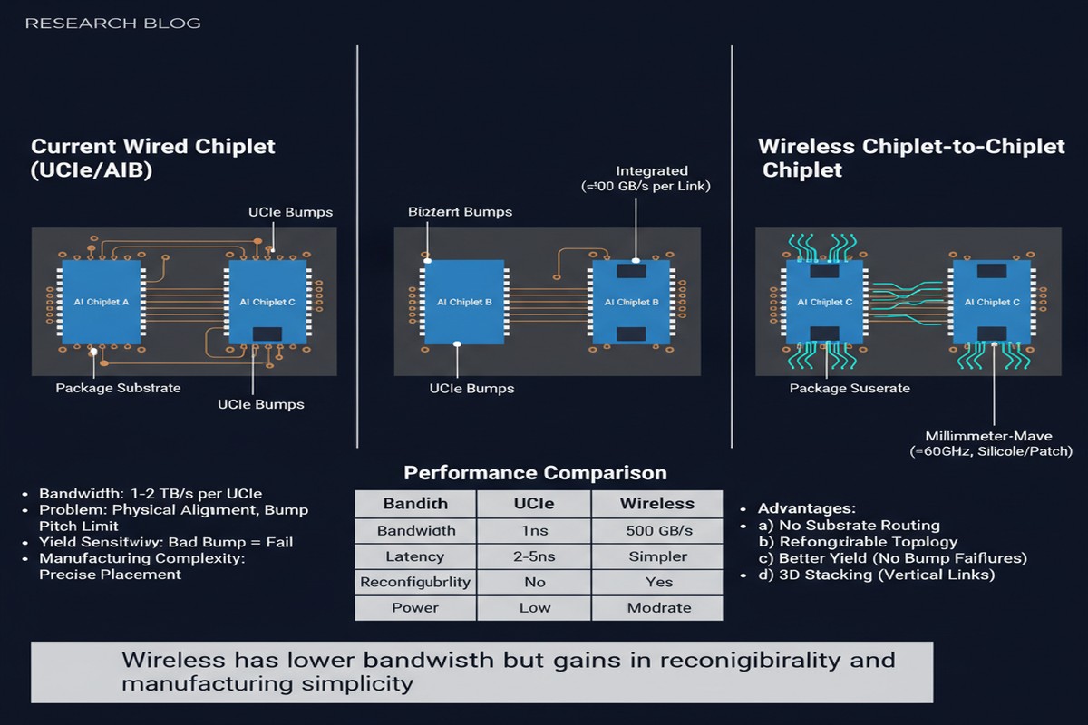
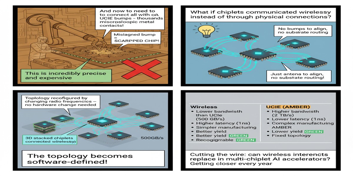
First, let me explain why anyone would even think about wireless inside a chip package. The problem is not bandwidth — today's die-to-die interconnects (UCIe, BoW, NVLink) can deliver hundreds of gigabytes per second per link. The problem is topology.
In a multi-chiplet package, the physical substrate constrains which chiplets can communicate directly. Chiplets that are not adjacent on the substrate must communicate through routing layers on the substrate — essentially traversing intermediate hops through the package. This adds latency and consumes routing resources on the substrate.
For AI workloads, this matters because the communication pattern is often not nearest-neighbor. In a transformer forward pass:
- The attention mechanism communicates across all sequence positions (global)
- Tensor parallel execution communicates across all GPU/chiplet replicas (all-reduce)
- Pipeline parallelism communicates between adjacent pipeline stages (nearest-neighbor)
All-reduce and global attention patterns require chiplets that may be physically far apart on the substrate to communicate efficiently. Routing these through multiple substrate hops adds latency at exactly the moments when AI workloads can least afford it — during synchronization barriers.
Wireless interconnects inside the package bypass the substrate routing constraint. A wireless link between chiplets on opposite sides of the package has the same physical latency as a wireless link between adjacent chiplets — distance within a centimeter-scale package barely matters at the frequencies used.
graph TD
    subgraph "Wired Multi-Chiplet Package"
    A[Chiplet 1] -->|substrate hop| B[Chiplet 2]
    B -->|substrate hop| C[Chiplet 3]
    A -.->|3 hops| C
    end

    subgraph "Wireless-Augmented Package"
    D[Chiplet 1] -->|wired| E[Chiplet 2]
    E -->|wired| F[Chiplet 3]
    D -->|wireless direct| F
    end

    style A fill:#faa,stroke:#c00
    style C fill:#faa,stroke:#c00
    style D fill:#afa,stroke:#0a0
    style F fill:#afa,stroke:#0a0
The Technology: mm-Wave and THz On-Package Communication
The paper uses mm-wave (millimeter-wave, 60-300 GHz) and terahertz (300 GHz - 3 THz) frequency bands for the wireless links. At these frequencies, antenna structures are small enough to integrate on-die or on the package substrate, and the data rates achievable approach those of wired die-to-die links.
This is not theoretical. On-chip wireless communication at 60 GHz has been demonstrated in silicon for over a decade. Companies including Intel, IBM, and various academic groups have published working implementations of wireless die-to-die links at chip scale. What's novel about this paper is applying the concept specifically to AI accelerator multi-chiplet workloads and quantifying the benefit for that specific application domain.
The wireless links in the paper's evaluation are not replacing wired links — they augment them. Wired links remain the primary high-bandwidth channel. The wireless links provide a low-latency, topology-flexible secondary channel for the specific traffic patterns that benefit from bypassing substrate routing.
flowchart LR
    subgraph "Communication Pattern"
    A[All-Reduce Traffic\nAll-to-All] --> B{Router}
    C[Local Tensor Traffic\nNearest-Neighbor] --> B
    B -->|Wired UCIe| D[Adjacent Chiplet]
    B -->|Wireless mm-Wave| E[Distant Chiplet\nDirect]
    end
    subgraph "Speedup"
    F[10% Average Speedup]
    G[20% Max on All-Reduce Workloads]
    end
Workload Analysis
The paper evaluates on six AI workload classes:
- Dense transformer inference (BERT, GPT variants)
- Vision transformer inference (ViT, DeiT)
- Sparse attention inference (models with sparse attention patterns)
- Training workloads (data parallel, tensor parallel)
- Mixture-of-Experts inference (MoE, with dynamic routing)
- Graph neural networks (GNN, with irregular communication)
The 10% average speedup and 20% peak speedup are aggregated across these workloads. MoE inference benefits most because MoE's expert routing creates irregular, long-range communication patterns that wired substrate routing handles poorly. GNNs show similar benefits for the same reason.
Dense transformers in tensor-parallel configuration benefit from the improved all-reduce performance. Data-parallel training shows smaller benefits because its communication patterns are already well-served by wired links.
Engineering Challenges
The paper is honest about the challenges, which I appreciate:
Interference management — Multiple wireless links within a package operating simultaneously can interfere. The paper discusses frequency-division and time-division schemes, but admits that interference remains a design challenge at high link densities.
Power consumption — Wireless transmitters consume power. The paper shows that the speedup benefits outweigh the additional power cost for the workloads that benefit, but the power budget for wireless infrastructure is non-trivial.
Antenna integration — Getting efficient antennas on-die or on-substrate in standard CMOS processes is not trivial. The paper assumes antenna designs that have been demonstrated in research but are not yet production-standard.
Security — Wireless signals can be intercepted. For AI accelerators processing proprietary models and sensitive data, this is a real concern that the paper mentions but does not fully address.
Why This Matters
The multi-chiplet packaging industry is in its early innings. UCIe standardization is ongoing. The design space for multi-chiplet AI accelerators is wide open. This paper contributes a genuine new dimension to that design space: topology-flexible communication through wireless links.
The 10-20% speedup range is meaningful but not transformative on its own. The real value of the wireless augmentation idea may be less about average-case performance improvement and more about enabling new packaging topologies. If wireless links allow chiplets to be arranged in configurations that optimize thermal dissipation or yield at the expense of substrate routing efficiency, and then wireless picks up the communication slack, you've expanded the feasible design space significantly.
For the most demanding all-reduce patterns in multi-GPU / multi-chiplet training, even a 20% speedup on that bottleneck can translate to meaningful reduction in training time and cost at scale.
My Take
I find this idea genuinely interesting and underexplored. The semiconductor industry has been so focused on pushing wired interconnect performance — more UCIe lanes, higher HBM bandwidth, better silicon interposers — that the alternative of wireless supplementation has received little serious attention in the AI hardware context.
The technical feasibility is not the main question — mm-wave on-chip wireless has been demonstrated convincingly. The question is whether the engineering overhead (interference management, power, antenna integration) is justified by the performance gains for specific AI workload patterns. The paper answers this affirmatively for all-reduce-heavy workloads, which happen to be among the most important workloads for LLM training.
My honest assessment: wireless inside a chip package will happen eventually, but probably not in the next generation. The standardization overhead is significant — you cannot add wireless links to a multi-chiplet design without coordinating antenna placement, frequency allocation, and protocol design across all chiplet vendors in the package. Given how long UCIe standardization has taken, adding wireless to the mix is a multi-year effort.
But the right moment to start thinking seriously about this technology is before you need it, not after. This paper does the service of establishing the performance potential early. When wireless die-to-die communication eventually appears in production silicon, this work will be part of the foundation.
Exploring the Potential of Wireless-enabled Multi-Chip AI Accelerators — arXiv:2501.17567, January 2025.