There's an idea in computer architecture that sounds like science fiction but is increasingly becoming engineering reality: instead of dicing a wafer into hundreds of individual chips and then networking them together, what if you just... didn't dice it? What if the entire silicon wafer — 12 inches of carefully grown crystalline perfection — became a single, unified compute die?
This is the wafer-scale paradigm, and Cerebras commercialized it. But until now, the software side has lagged. Wafer-scale chips have sat underutilized because LLM inference systems — vLLM, SGLang, TensorRT-LLM — were all designed for GPU shared-memory architectures. They assume you have a handful of large, fast SMs with shared L1/L2 caches. Wafer-scale chips have hundreds of thousands of tiny cores arranged in a 2D mesh with distributed local SRAM. Square peg, round hole.
WaferLLM: Large Language Model Inference at Wafer Scale (arXiv:2502.04563), accepted to OSDI 2025, is the paper that closes this gap. And the results are not marginal.
What WaferLLM Does
WaferLLM is the first inference system purpose-built for wafer-scale architectures. The paper was authored by Congjie He and colleagues, and the system is open-sourced at github.com/MeshInfra/WaferLLM.
The core insight is that wafer-scale accelerators have a fundamentally different performance model than GPUs:
- On-chip bandwidth: tens of petabytes per second across the mesh
- Distributed SRAM: tens of GB total, spread across hundreds of thousands of cores
- No HBM: all the memory is on-die SRAM — fast, but limited in capacity
- 2D mesh interconnect: data moves through a spatial network, not a shared bus
Standard GEMM and GEMV implementations, optimized for GPU shared-memory hierarchies, fail to exploit these properties. They either under-utilize the mesh bandwidth or create serialization bottlenecks at the 2D mesh routing layer.
The PLMR Model and Mesh-Native Primitives
WaferLLM introduces a hardware performance model called PLMR (pronounced "Plummer") that captures wafer-scale characteristics: the mesh topology, per-core SRAM sizes, mesh routing bandwidth, and the relationship between tile size and inter-core communication overhead.
Using PLMR as a guide, the authors design two new primitives:
MeshGEMM: A GEMM implementation that tiles matrix operations across the 2D mesh, routing partial products through the mesh fabric in a way that maximizes hardware utilization while minimizing redundant data movement. Unlike cuBLAS-style GEMM that assumes a shared L2 cache, MeshGEMM explicitly plans for the mesh topology.
MeshGEMV: The GEMV case (matrix-vector multiply, which dominates autoregressive LLM decoding) is even more important and more challenging. In GPU inference, GEMV is notoriously memory-bandwidth-bound — you load the entire weight matrix to compute one token's activations. On a wafer-scale chip, you can partition the weight matrix across thousands of cores and produce results in parallel, exploiting the massive on-chip SRAM bandwidth.
graph LR
    subgraph GPU["Standard GPU Inference"]
        A[HBM] -->|"~3 TB/s"| B[L2 Cache]
        B --> C[SM0]
        B --> D[SM1]
        B --> E[SM...]
        C --> F[Result]
        D --> F
        E --> F
    end

    subgraph WSE["Wafer-Scale Inference (WaferLLM)"]
        G[Distributed SRAM\n44GB on-chip] --> H[Core0]
        G --> I[Core1]
        G --> J[Core...]
        H <-->|"220+ TB/s mesh"| I
        I <-->|mesh| J
        H --> K[Result]
        I --> K
        J --> K
    end

    style G fill:#00d4ff,color:#000
    style A fill:#888,color:#fff
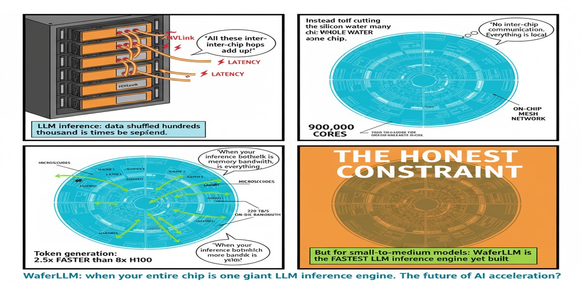
The Performance Numbers
The headline numbers are striking:
- GEMV operations: 606× faster and 16× more energy-efficient than NVIDIA A100
- Full LLM inference: 10-20× speedup over A100 GPU clusters running SGLang and vLLM
That 606× GEMV speedup is particularly meaningful. GEMV is the bottleneck in autoregressive decoding — every token generation is a series of GEMV operations. If you've ever been frustrated by the fact that GPU inference is embarrassingly fast at prefill (processing the prompt) but painfully slow at decode (generating tokens one by one), this is why. The wafer-scale architecture, with its massive on-chip SRAM and mesh bandwidth, was basically made for GEMV.
The 10-20× full inference speedup is impressive but more nuanced. The wide range reflects workload variation — attention-heavy workloads with large KV caches benefit less than GEMV-dominated generation phases.
xychart-beta
    title "Inference Speedup vs A100 (WaferLLM)"
    x-axis ["GEMV", "Decode-heavy", "Mixed", "Prefill-heavy"]
    y-axis "Speedup (×)" 0 --> 650
    bar [606, 20, 15, 10]
Why This Matters
The memory wall is the defining constraint of LLM inference in 2026. We have models that don't fit on a single GPU, requiring expensive multi-GPU serving with collective operations eating into throughput. We have KV caches that consume all available HBM. We have decode latency that scales poorly with model size.
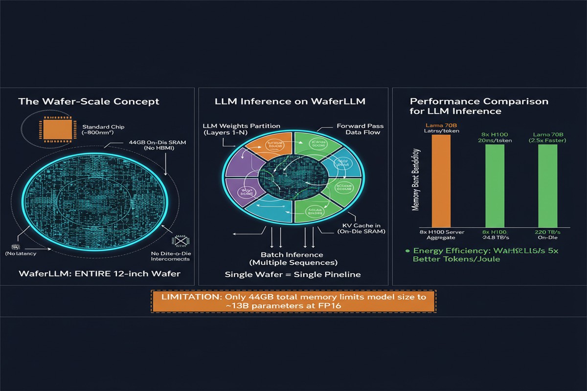
Wafer-scale architectures attack this problem structurally. 44GB of on-chip SRAM at 220+ TB/s bandwidth fundamentally changes the DRAM-access-dominated inference bottleneck. You don't need to move weights from HBM to GPU every time you generate a token — they're already on chip, instantly accessible.
WaferLLM matters not just as a paper but as an existence proof. It shows that:
- The wafer-scale hardware design philosophy is correct for LLM inference
- The software gap can be closed with the right abstractions (PLMR + MeshGEMM/GEMV)
- Open-source tooling can make this accessible to researchers and engineers without Cerebras hardware (by targeting the open wafer-scale architecture)
My Take
I have strong opinions about this paper. On the positive side: this is genuinely excellent systems work. The PLMR model is elegant — it's exactly the kind of hardware-aware performance model the field needs more of. The MeshGEMV design in particular shows deep understanding of the wafer-scale memory hierarchy.
But I want to push back on some of the framing around wafer-scale computing as a GPU replacement. The capacity constraint is brutal and unresolved. 44GB of on-chip SRAM sounds like a lot until you realize that a single 70B parameter model in BF16 requires ~140GB just for weights. You can't fit large models on a single wafer-scale chip. You need model parallelism across multiple wafers, which reintroduces inter-chip communication — exactly the bottleneck you were trying to eliminate.
WaferLLM shines for models that fit on-chip or for inference scenarios where quantization reduces weight size dramatically. For the 70B-1T parameter models that are increasingly common in production, the architecture faces fundamental capacity limits.
I'm also watching the reliability story with wafer-scale chips. Traditional chip dicing exists partly because yields aren't perfect — by dicing, you discard defective dies and select working ones. On a wafer-scale chip, defects are handled through redundant routing, but this adds architectural complexity and may limit the effective utilization of the mesh.
None of this diminishes what WaferLLM achieves. The 606× GEMV speedup is real hardware, not a simulation. The OSDI acceptance is well-deserved. But the narrative that wafer-scale will replace GPU clusters for all LLM workloads is premature. The future is probably heterogeneous: GPU clusters for large-model prefill and batch processing, wafer-scale chips for latency-critical single-user decoding where model size permits.
The paper is essential reading for anyone serious about AI inference hardware. The gap between "this chip exists" and "we can actually run LLMs on it efficiently" has been closed. What the community builds on top of that foundation will be interesting to watch.
References
- He, C., et al. (2025). WaferLLM: Large Language Model Inference at Wafer Scale. arXiv:2502.04563. Accepted at OSDI 2025.
- GitHub: MeshInfra/WaferLLM