The AI chip wars have a dominant narrative: NVIDIA makes the hardware, everyone else makes announcements. This is unfair, and a March 2025 arXiv paper is one of the more honest attempts I've seen to challenge it.
A Comparison of the Cerebras Wafer-Scale Integration Technology with Nvidia GPU-based Systems for Artificial Intelligence (arXiv:2503.11698) is exactly what it claims to be: a head-to-head technical comparison of Cerebras' WSE-3 architecture against NVIDIA's H100 and B200. It doesn't declare a winner. It lays out the trade-offs with specificity and lets the data speak.
This is the kind of paper the AI hardware field desperately needs more of.
What Is WSE-3?
Before comparing, you need to understand what Cerebras actually built. The WSE-3 is not a GPU. It is not a GPU with more cores. It is a fundamentally different architectural philosophy instantiated in silicon.
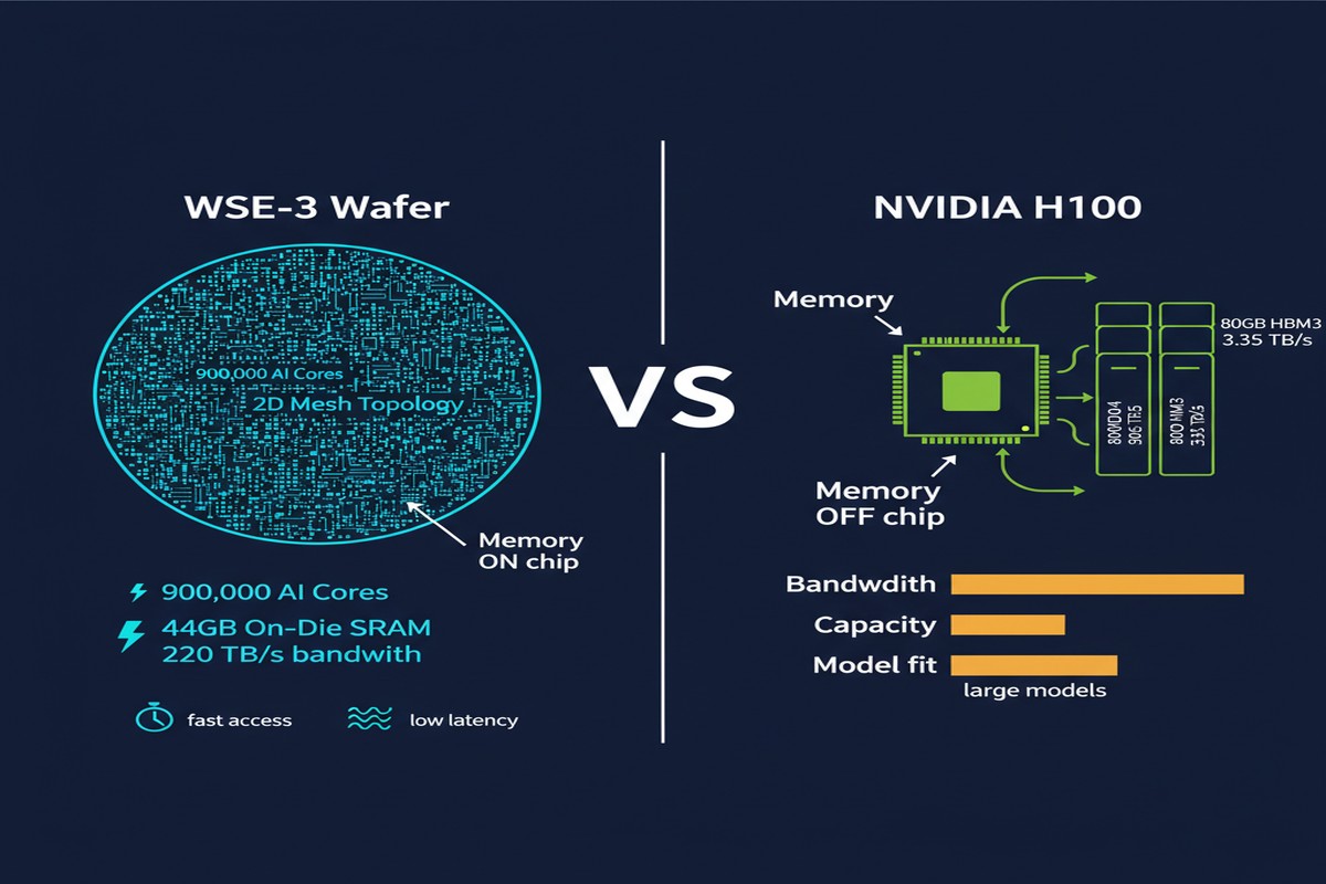
The WSE-3 packs 900,000 AI cores onto a single 12-inch silicon wafer. These cores are arranged in a 2D mesh with 220+ TB/s of on-chip SRAM bandwidth and 44GB of total on-die SRAM. For context, an H100 has 132 SMs, 80GB of HBM3 off-chip memory, and ~3.35 TB/s HBM bandwidth. The bandwidth gap — 220 TB/s vs 3.35 TB/s — is the architectural headline, and everything flows from it.
The tradeoff: WSE-3 has no HBM. All 44GB is on-die. This gives you extraordinary bandwidth for data that fits on-chip, and a hard capacity wall for data that doesn't.
graph TD
    subgraph WSE3["Cerebras WSE-3"]
        A["900K AI Cores\n2D Mesh Topology"] --> B["44GB On-Die SRAM\n220+ TB/s bandwidth"]
        A --> C["~125 PFLOPs\nsparse half-precision"]
    end

    subgraph H100["NVIDIA H100 SXM5"]
        D["132 SMs\nShared Memory Model"] --> E["80GB HBM3\n~3.35 TB/s bandwidth"]
        D --> F["~2 PFLOPs\nBF16 dense"]
    end

    subgraph B200["NVIDIA B200"]
        G["192 SMs + TMEM\n5th Gen Tensor Cores"] --> H["192GB HBM3e\n~8 TB/s bandwidth"]
        G --> I["~9 PFLOPs\nFP8 dense"]
    end

    style B fill:#00d4ff,color:#000
    style E fill:#76b900,color:#fff
    style H fill:#76b900,color:#fff
What the Paper Finds
The comparison paper evaluates several workload categories:
Training Performance
For training workloads, the WSE-3 shows strong advantages on:
- Small-to-medium model training where model weights fit comfortably in 44GB on-die SRAM
- High-iteration training where gradient updates benefit from the mesh bandwidth
- Sparse training where 900K cores can exploit sparsity at fine granularity
The paper reports that for certain training configurations, WSE-3 can achieve better performance-per-dollar than H100 clusters when factoring in interconnect costs. The key qualifier: when the model fits on-die.
Inference Performance
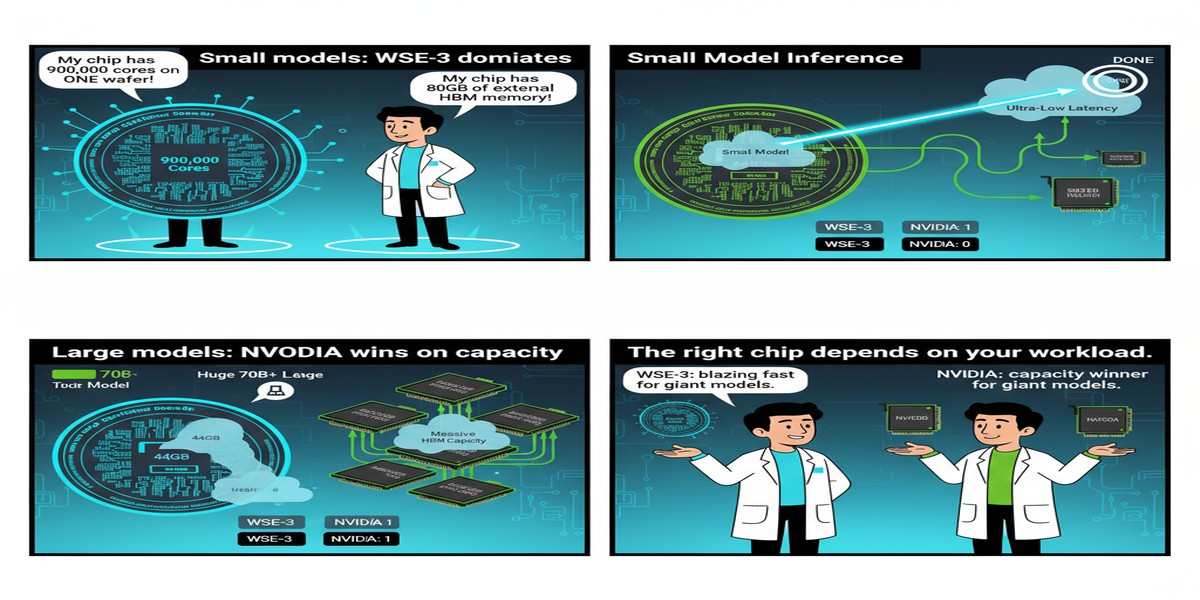
This is where the comparison gets interesting. For inference:
- Small model inference (sub-7B): WSE-3 can achieve extraordinary throughput and latency, leveraging on-chip SRAM to eliminate HBM round trips
- Large model inference (70B+): This is where the architecture shows strain. With only 44GB on-die, you can't fit large models without aggressive quantization or model sharding across multiple WSEs
- Batch inference: H100 and B200 win here. Their HBM provides the capacity to cache large KV stores and serve many concurrent users
Energy Efficiency
The paper's energy efficiency data is one of its most valuable contributions. WSE-3 trades raw FLOPS per watt for bandwidth per watt — which turns out to be the right metric for memory-bound workloads. For bandwidth-bound operations (GEMV-dominated decoding, embedding lookups), WSE-3's efficiency advantage is significant.
The Memory Capacity Problem
I want to be direct about the elephant in the room that the paper addresses head-on: 44GB of on-die SRAM is both WSE-3's greatest strength and its most significant limitation.
Llama 3.1 70B requires approximately 140GB in BF16. Llama 3.1 405B requires ~810GB. Even with 4-bit quantization, 70B needs ~35GB — just barely squeezable into 44GB with nothing left for KV cache. 405B quantized? Still ~200GB. You're looking at multi-WSE setups with inter-chip communication — exactly what wafer-scale was supposed to avoid.
The counter-argument: Cerebras' CS-3 systems are designed for multi-chip scaling, and the interconnect bandwidth between CS-3 systems is higher than typical multi-GPU setups. But the architectural elegance of "one big chip, no interconnects" degrades as you scale beyond single-chip capacity.
flowchart TD
    A[Model Size] --> B{Fits in 44GB?}
    B -->|Yes ≤7B dense| C[WSE-3 Wins\nExtraordinary speed]
    B -->|Borderline 7-13B quantized| D[WSE-3 Competitive\nWith tuning]
    B -->|No 70B+| E[Multi-WSE Required\nNVIDIA advantage in capacity]

    C --> F[Single chip inference\nNo interconnect overhead]
    D --> G[Aggressive INT4/INT8\nLimited KV cache]
    E --> H[H100/B200 clusters\nHBM capacity advantage]

    style C fill:#00d4ff,color:#000
    style E fill:#76b900,color:#fff
Why This Matters
This paper matters for reasons beyond its benchmark data. It represents a serious attempt to give the AI hardware community an honest, academically rigorous comparison tool. Too much of the discourse around AI chips is vendor-driven marketing or breathless tech journalism. Neither helps you decide what to put in your datacenter.
The broader lesson from this comparison: there is no universal "best" AI chip. The right hardware depends critically on:
- Model size: Does your target model fit on-chip?
- Workload type: Training vs inference, batch vs real-time, compute-bound vs bandwidth-bound
- Scale: Single-chip vs multi-chip, small cluster vs hyperscale
- Cost model: Capital cost vs operational cost vs cost per token
For organizations training smaller, custom models (sub-10B, which describes a huge fraction of enterprise AI), WSE-3 deserves serious evaluation. For hyperscale LLM serving with frontier-sized models, NVIDIA's ecosystem maturity and HBM capacity make it the safer choice — for now.
My Take
I'll say something that might surprise you: I think Cerebras has built something genuinely impressive, and the mainstream AI community underrates them because the CUDA ecosystem is so deeply entrenched.
The WSE-3's bandwidth numbers are not marketing fiction. 220 TB/s on-chip bandwidth is physically real and architecturally transformative for the right workloads. The problem isn't the chip — it's the narrative positioning. Cerebras wants to compete with H100 at everything, and that's a losing battle. They should be laser-focused on the use cases where WSE-3 dominates: low-latency inference for mid-size models, high-throughput training for medium-scale experiments, and research organizations that value rapid iteration over raw model scale.
The paper's comparison shows that WSE-3 can legitimately beat H100 on specific workloads. That should be the story. Instead, the company tries to compete on headline FLOPS numbers where NVIDIA's manufacturing scale gives them a permanent advantage.
I also want to flag a limitation of this comparison paper: the B200 data is limited. The B200 was newer at time of writing, and some B200 benchmarks rely on projected rather than measured performance. The comparison will need updating as Blackwell systems become more widely available.
The competition between wafer-scale and GPU architectures is healthy for the industry. Every paper like this one — honest, rigorous, comparative — moves us toward better hardware decisions and more productive architectural debate. More of this, please.
References
- Jarmusch, A., et al. (2025). A Comparison of the Cerebras Wafer-Scale Integration Technology with Nvidia GPU-based Systems for Artificial Intelligence. arXiv:2503.11698.
- Cerebras Systems. (2024). CS-3 / WSE-3 Technical Specifications. Cerebras Technical Reports.